SUBLEQ - Part I
This project has been featured on HackADay on 7/27/2011.
2022: The content is presented as originally written with slight annotations for readability.
Introduction
An OISC (one instruction set computer) is an extremely simplified computer architecture. Instead of a fully-featured instruction set (also known as a complex instruction set), a OISC has only one operation; it is the RISC approach to computing taken to the extreme.
A SUBLEQ computer based on the OISC model has only one instruction, eliminating the need for an opcode field in the instruction. The model specified below has a datapath width of 8 bits, but the instruction word is 24 bits wide, and is formatted in terms of memory locations it addresses.
The SUbtract and Branch if Less or EQual instruction is a fairly straightforward mathematical operation; tt extracts the integers stored in memory at location[a] and location[b], subtracts the value of location [b] from location[a] and writes the result back into location[b]. If the result is an integer less than or equal to zero, it jumps to the instruction location pointed to by c, if not it continues on to the next instruction.
The SUBLEQ computer will be modeled in Xilinx ISE Webpack 13.2 using a schematic as the top-level module. It would be far easier to implement it as one Verilog module, but keeping it simple is the objective here.
Why an OISC? It's the easiest model of a computer to build from components and still be understandable to a reader with only little experience in computer engineering.
Design
This implementation of the SUBLEQ computer will have two stages per instruction, fetch and execute.
Fetch: In this state, the computer will fetch the next instruction from the instruction memory (from hereon to be known as the instruction ROM) pointed to by the program counter PC and store it in the instruction register IR.
Execute: the computer would use the operands of the instruction to access the data memory (RAM) and extract the operands, subtract operand[b] from operand[a], and store the result in RAM location b. If the result is <= 0, the PC is set to c (from the instruction), if not, PC is incremented.
All integers will be stored in two's complement format. Since the SUBLEQ operation requires subtraction and the possibility that the result will be negative, the computer will be using two's complement integers exclusively (a detailed first look at two's complement notation is available.)
Implementation
The ALU
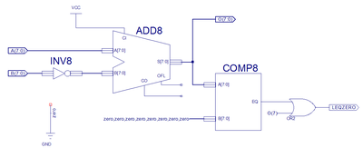
The Arithmetic and Logic Unit is an integral part of a modern computer. For the purposes of the SUBLEQ computer, the design of the ALU is fairly straightforward; it only has to perform the subtraction operation and to signal that the answer is negative or zero. As such, it will be a purely combinational logic element.
The implementation uses a ripple-carry adder (ADD8 (8-bit adder)) element to illustrate the ease of performing subtraction in the two's complement format. Simply invert all the bits of the minuend using the INV8 and add it to the subtrahend and add in 1 (the carry-in input is wired to +VCC to show that the carry in is permanent - the ALU only does subtraction and comparison.) Overflows are disregarded for the sake of simplicity. The output of the subtraction operation is compared to 0b00000000 by the comparator (COMP8) to check if it's zero. A simple OR gate ensures that LEQZERO will only be active when either the output is zero, or the MSB of the answer is positive. (A set MSB will indicate that the output is a negative integer.)
Testing the ALU is rather simple with a Verilog test fixture. Running the simulation for about 0.2ms in simulation time (or well over 2 million samples) satisfies that there are no errors in logic.
module alu_alu_sch_tb();

// Inputs
   reg [7:0] B;
   reg [7:0] A;
    reg CLK;

// Output
   wire LEQZERO;
   wire [7:0] O;

// Bidirs

// Instantiate the UUT
   alu UUT (
        .B(B),
        .A(A),
        .LEQZERO(LEQZERO),
        .O(O)
   );

/* Initialize Inputs. Start A and B from different   values to achieve the full coverage.*/
      initial begin
        B = 0;
        A = 8'hf0;
        CLK=0;
        end

/*automated testing block, signals only if there is an error.*/

    always @(posedge CLK)
    begin
    A = A+1;
    B = B+1;
    #1;
/*if the output is NOT the difference between A and B, log an error*/
if (~(O == (A - B)) ||
    ~(LEQZERO == (O[7] | (O==8'b0))))

        begin
        $display("error! A=%b B=%b O=%b", A, B, O);
        end
    end


/*generate a clock signal for the testing block to keep track of time.*/
    always begin
    #10 CLK=~CLK;
    end


endmodule
Multiplexer
This humble piece of logic performs a simple yet critical task. When the select line is HIGH, the output values reflects the input values at port A continuously. When the select line is LOW, the output values mirror the inputs at port B (read more about the mux at Wikipedia.)
`timescale 1ns / 1ps
module mux_2x1(
    input [7:0] A,
    input [7:0] B,
    input sel,
    output [7:0] out
    );
assign out = (sel)? A: B;

endmodule
Program Counter (PC)
This register keeps track of where in the ROM the current instruction is located. Updating the PC is done only when the execution of the current instruction is complete.
`timescale 1ns / 1ps
module programcounter(
     input WE,
     input RST,
     input CLK,
     output [7:0] PC
    );
reg [7:0] PCinternal;

always @(posedge CLK)
//on the positive edge of the clock
begin

    //if reset signal is asserted, go back to
    //Instruction 1
    //(instruction 0 is a HLT instruction)

    if (RST)
    PCinternal <= 8'b1;

    if (WE)
    //if WE is held high, update the value of PC
    PCinternal <= PCnew;
end

//PC (the output) mirrors the internal registers.
assign PC =PCinternal;

endmodule
Instruction Register (IR)
This register fetches the current instruction from the ROM whenever the EN line is asserted and latches the value until told to reset (RST) or until EN is asserted again.
module ireg_24(
    input [23:0] instr_in,
    input EN,
    output reg [23:0] instr_out,
     input CLK,
     input RST
    );

/*on the positive edge of the clock,
or if RST is triggered*/

always @(posedge CLK or posedge EN) begin
if (RST)
// highest priority
instr_out <=24'b0;
else if (EN)
 instr_out <= instr_in;
end


endmodule
Dual Port RAM
This is a Verilog implementation of a dual port RAM, allowing two RAM locations to be read simultaneously. Only one write can be done at once, and only when WE is held HIGH, and there are 256 bytes of RAM. The initial block initializes the RAM with values read in from data.ram.
module dp_ram(
    input [7:0] addrA,
    input [7:0] addrB,
    output [7:0] dataA,
    output [7:0] dataB,
    input [7:0] addrC,
    input [7:0] dataC,
    input WE,
     input CLK
    );

reg [7:0] selA, selB;
reg [7:0] MEM [0:255];   //255 memory entries

initial begin
$readmemh("data.ram", MEM);
end

always @(posedge CLK)
begin
if (WE)                  //WE strobe on positive edge of  clock?
MEM[addrC] <= dataC;     //store DataIn at mem[address C]

selA <= addrA;           //update the addresses
selB <= addrB;
end

assign dataA = REGS[selA];
assign dataB = REGS[selB];

/*connect the outputs of the inferred BRAM
to the outputs DataOutA and DataOutB*/

endmodule
Instruction ROM
The instruction ROM holds all the instructions necessary for the SUBLEQ computer to work. Instead of typing them in by hand, the initial begin block reads in the contents of a text hex file into the registers, which is very convenient. The operational features of the ROM mirrors that of the RAM; it reads the instruction at the location pointed to by addr.
module rom_256(
    input [7:0] addr,
    input CLK,
    output [23:0] data
    );
reg [23:0] IMEM [0:255]; //256 instructions

initial begin                 //load instructions into ROM from a hex file
$readmemh("data.rom",IMEM);
end

always @(posedge CLK)
begin
data = IMEM[addr];        //output the value at memory[addr]
end

endmodule
Sequencer
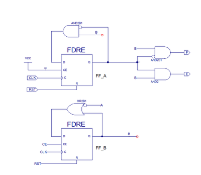
To arbitrate the rest of the system, the sequencer cycles through the two states fetch and execute in rapid succession, using two D-flip flops to satisfy the need for three defined states (and one unused state.)
Asserting RST at any point in time will reset both flip flops to zero, so STATE0 is defined as 0b00. The need for a separate post-reset state is to allow the next state (FETCH) to run for one complete clock cycle. Each flipflop is fed a combination of logic known as the next state equations (for more information, breeze through synchronous logic.)
At the first positive CLK edge after RST, the sequencer will then transition through STATE1 (0b01) and STATE2 (0b10), looping back to STATE1 and continuing indefinitely. STATE3 (0b11) is unused, however, if by accident (or random gamma ray strike) the state machine transitions to STATE3, it will then transition back to STATE0 and then resume its normal cycle.
Assembly
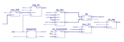
Now that all the components have been introduced, here's how they fit together:
PC_incrementer is a simple module that increments the input by 1 every time the enable signal is asserted. The multiplexer selects either the incremented PC or the c operand of the instruction depending on the value of LEQZERO. Remember that LEQZERO will be asserted only if the output of the ALU is less than or equal to zero, so that the value passed to the new value of PC will be operand c if LEQZERO is HIGH.
Other than that, the rest of the layout is self-explanatory. ireg_24 only stores the output of the next instruction when FETCH is HIGH, and therefore there is only one instruction per CPU cycle. The RAM is hardwired to write the answer of RAM[a] - RAM[b] back into RAM[b], and only do so on the rising edge of CLK.
This concludes part I of the two-part howto on synthesizing your own one-instruction computer. Part II will be coming soon, and it will address how to write a simple program for your computer design -- and how to run it.


Comments
Comments powered by Disqus